MIT PROCESSING , Made in Taiwan


smtekco

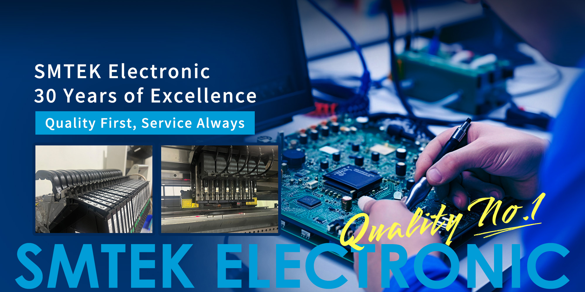
SMTEK ELECTRONIC INDUSTRIES CO., LTD.-SMT,Taiwan SMT,
店家文章分享
What is PCB Layout?
What is PCB Layout?

PCB Layout, or Printed Circuit Board Layout, refers to the process of arranging and connecting electronic components on a printed circuit board (PCB) based on the schematic design. PCB layout is a critical stage in PCB design and is typically the most time-consuming part of the entire process.
Goals of PCB Layout
Meet the requirements of the schematic design
Ensure the performance and reliability of the PCB
Reduce PCB manufacturing costs
Typical PCB Layout Process
Determine PCB Size: Define the PCB dimensions according to the schematic design requirements.
Component Creation: any new components required for the design.
Component Placement: Position components on the PCB.
Constraint Setup: Configure physical, spacing, and electrical constraints (Layout Rules).
Routing: Design the interconnections between components.
DRC Check: Perform Design Rule Checks (DRC) to ensure the layout meets all design rules.
Gerber Generation: Generate Gerber files used for PCB manufacturing.
Key Considerations in PCB Layout
Electrical Performance: The layout must meet schematic requirements to ensure proper electrical functionality.
EMC Performance: Electromagnetic compatibility (EMC) must be considered to minimize electromagnetic radiation and improve noise immunity.
Thermal Performance: Proper heat dissipation must be planned to prevent overheating during operation.
Manufacturability: The layout should support efficient production and help reduce manufacturing costs.
Serviceability: The PCB should be designed for easy maintenance and repair.
PCB layout is a complex technical skill that requires specialized knowledge and extensive experience to ensure a reliable final product. If you require PCB layout services, it is recommended to use professional PCB layout software and work with experienced PCB layout engineers—or collaborate with a qualified PCB layout service provider.
其它相關店家資訊


免責聲明本網站僅提供製造業公司資訊參考平台, 並不涉入其中任何諮詢、交易。本網站對各該製造業公司相關資訊亦不作任何實質或形式上之審查。就本網站中所載一切製造業公司的資訊、文字、照片、圖形 、產權、廣告內容、或其他資料(以下簡稱『內容』),無論其為公開張貼或私下傳送,若有不實或違法情事,均為『內容』提供者之責任,本站概不負責也不承擔任何法律責任